- 您现在的位置:买卖IC网 > Sheet目录329 > IDT70T653MS12BCI (IDT, Integrated Device Technology Inc)IC SRAM 18MBIT 12NS 256BGA
IDT70T653M
High-Speed 2.5V 512K x 36 Asynchronous Dual-Port Static RAM
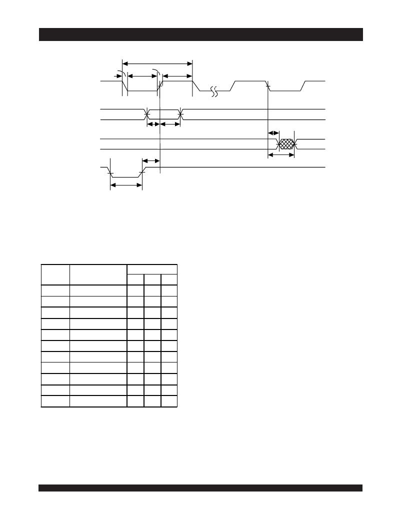
JTAG Timing Specifications
t JCYC
Industrial and Commercial Temperature Ranges
t JF
t JCL
t JR
t JCH
TCK
Device Inputs (1) /
TDI/TMS
Device Outputs (2) /
t JS
t JH
t JDC
TDO
TRST
t JRSR
t JCD
x
5679 drw 24
t JRST
NOTES:
1. Device inputs = All device inputs except TDI, TMS, TCK and TRST .
2. Device outputs = All device outputs except TDO.
JTAG AC Electrical
Characteristics (1,2,3,4,5)
70T653M
3
3
Symbol
t JCYC
t JCH
t JCL
t JR
t JF
t JRST
Parameter
JTAG Clock Input Period
JTAG Clock HIGH
JTAG Clock Low
JTAG Clock Rise Time
JTAG Clock Fall Time
JTAG Reset
Min.
100
40
40
____
____
50
Max.
____
____
____
(1)
(1)
____
Units
ns
ns
ns
ns
ns
ns
t JRSR
t JCD
JTAG Reset Recovery
JTAG Data Output
50
____
____
25
ns
ns
NOTES:
1. Guaranteed by design.
2. 30pF loading on external output signals.
t JDC
t JS
t JH
JTAG Data Output Hold
JTAG Setup
JTAG Hold
0
15
15
____
____
____
ns
ns
ns
3. Refer to AC Electrical Test Conditions stated earlier in this document.
4. JTAG operations occur at one speed (10MHz). The base device may run at any
speed specified in this datasheet.
5. JTAG cannot be tested in sleep mode.
5679 tbl 20
22
发布紧急采购,3分钟左右您将得到回复。
相关PDF资料
IDT70V05L55G
IC SRAM 64KBIT 55NS 68PGA
IDT70V06L55G
IC SRAM 128KBIT 55NS 68PGA
IDT70V07L35G
IC SRAM 256KBIT 35NS 68PGA
IDT70V08S15PF
IC SRAM 512KBIT 15NS 100TQFP
IDT70V09L20PFI
IC SRAM 1MBIT 20NS 100TQFP
IDT70V18L20PFI
IC SRAM 576KBIT 20NS 100TQFP
IDT70V25L55G
IC SRAM 128KBIT 55NS 84PGA
IDT70V261L25PFGI
IC SRAM 256KBIT 25NS 100TQFP
相关代理商/技术参数
IDT70T653MS12BCI8
功能描述:IC SRAM 18MBIT 12NS 256BGA RoHS:否 类别:集成电路 (IC) >> 存储器 系列:- 标准包装:3,000 系列:- 格式 - 存储器:EEPROMs - 串行 存储器类型:EEPROM 存储容量:8K (1K x 8) 速度:400kHz 接口:I²C,2 线串口 电源电压:1.7 V ~ 5.5 V 工作温度:-40°C ~ 85°C 封装/外壳:8-SOIC(0.154",3.90mm 宽) 供应商设备封装:8-SOIC 包装:带卷 (TR)
IDT70T653MS15BC
功能描述:IC SRAM 18MBIT 15NS 256BGA RoHS:否 类别:集成电路 (IC) >> 存储器 系列:- 标准包装:3,000 系列:- 格式 - 存储器:EEPROMs - 串行 存储器类型:EEPROM 存储容量:8K (1K x 8) 速度:400kHz 接口:I²C,2 线串口 电源电压:1.7 V ~ 5.5 V 工作温度:-40°C ~ 85°C 封装/外壳:8-SOIC(0.154",3.90mm 宽) 供应商设备封装:8-SOIC 包装:带卷 (TR)
IDT70T653MS15BC8
功能描述:IC SRAM 18MBIT 15NS 256BGA RoHS:否 类别:集成电路 (IC) >> 存储器 系列:- 标准包装:3,000 系列:- 格式 - 存储器:EEPROMs - 串行 存储器类型:EEPROM 存储容量:8K (1K x 8) 速度:400kHz 接口:I²C,2 线串口 电源电压:1.7 V ~ 5.5 V 工作温度:-40°C ~ 85°C 封装/外壳:8-SOIC(0.154",3.90mm 宽) 供应商设备封装:8-SOIC 包装:带卷 (TR)
IDT70T659S10BC
功能描述:IC SRAM 4MBIT 10NS 256BGA RoHS:否 类别:集成电路 (IC) >> 存储器 系列:- 标准包装:3,000 系列:- 格式 - 存储器:EEPROMs - 串行 存储器类型:EEPROM 存储容量:8K (1K x 8) 速度:400kHz 接口:I²C,2 线串口 电源电压:1.7 V ~ 5.5 V 工作温度:-40°C ~ 85°C 封装/外壳:8-SOIC(0.154",3.90mm 宽) 供应商设备封装:8-SOIC 包装:带卷 (TR)
IDT70T659S10BC8
功能描述:IC SRAM 4MBIT 10NS 256BGA RoHS:否 类别:集成电路 (IC) >> 存储器 系列:- 标准包装:3,000 系列:- 格式 - 存储器:EEPROMs - 串行 存储器类型:EEPROM 存储容量:8K (1K x 8) 速度:400kHz 接口:I²C,2 线串口 电源电压:1.7 V ~ 5.5 V 工作温度:-40°C ~ 85°C 封装/外壳:8-SOIC(0.154",3.90mm 宽) 供应商设备封装:8-SOIC 包装:带卷 (TR)
IDT70T659S10BCI
功能描述:IC SRAM 4MBIT 10NS 256BGA RoHS:否 类别:集成电路 (IC) >> 存储器 系列:- 标准包装:3,000 系列:- 格式 - 存储器:EEPROMs - 串行 存储器类型:EEPROM 存储容量:8K (1K x 8) 速度:400kHz 接口:I²C,2 线串口 电源电压:1.7 V ~ 5.5 V 工作温度:-40°C ~ 85°C 封装/外壳:8-SOIC(0.154",3.90mm 宽) 供应商设备封装:8-SOIC 包装:带卷 (TR)
IDT70T659S10BCI8
功能描述:IC SRAM 4MBIT 10NS 256BGA RoHS:否 类别:集成电路 (IC) >> 存储器 系列:- 标准包装:3,000 系列:- 格式 - 存储器:EEPROMs - 串行 存储器类型:EEPROM 存储容量:8K (1K x 8) 速度:400kHz 接口:I²C,2 线串口 电源电压:1.7 V ~ 5.5 V 工作温度:-40°C ~ 85°C 封装/外壳:8-SOIC(0.154",3.90mm 宽) 供应商设备封装:8-SOIC 包装:带卷 (TR)
IDT70T659S10BF
功能描述:IC SRAM 4MBIT 10NS 208FBGA RoHS:否 类别:集成电路 (IC) >> 存储器 系列:- 标准包装:3,000 系列:- 格式 - 存储器:EEPROMs - 串行 存储器类型:EEPROM 存储容量:8K (1K x 8) 速度:400kHz 接口:I²C,2 线串口 电源电压:1.7 V ~ 5.5 V 工作温度:-40°C ~ 85°C 封装/外壳:8-SOIC(0.154",3.90mm 宽) 供应商设备封装:8-SOIC 包装:带卷 (TR)
